- 您现在的位置:买卖IC网 > Sheet目录321 > DS1230WP-150+ (Maxim Integrated Products)IC NVSRAM 256KBIT 150NS 34PCM
�� �
�
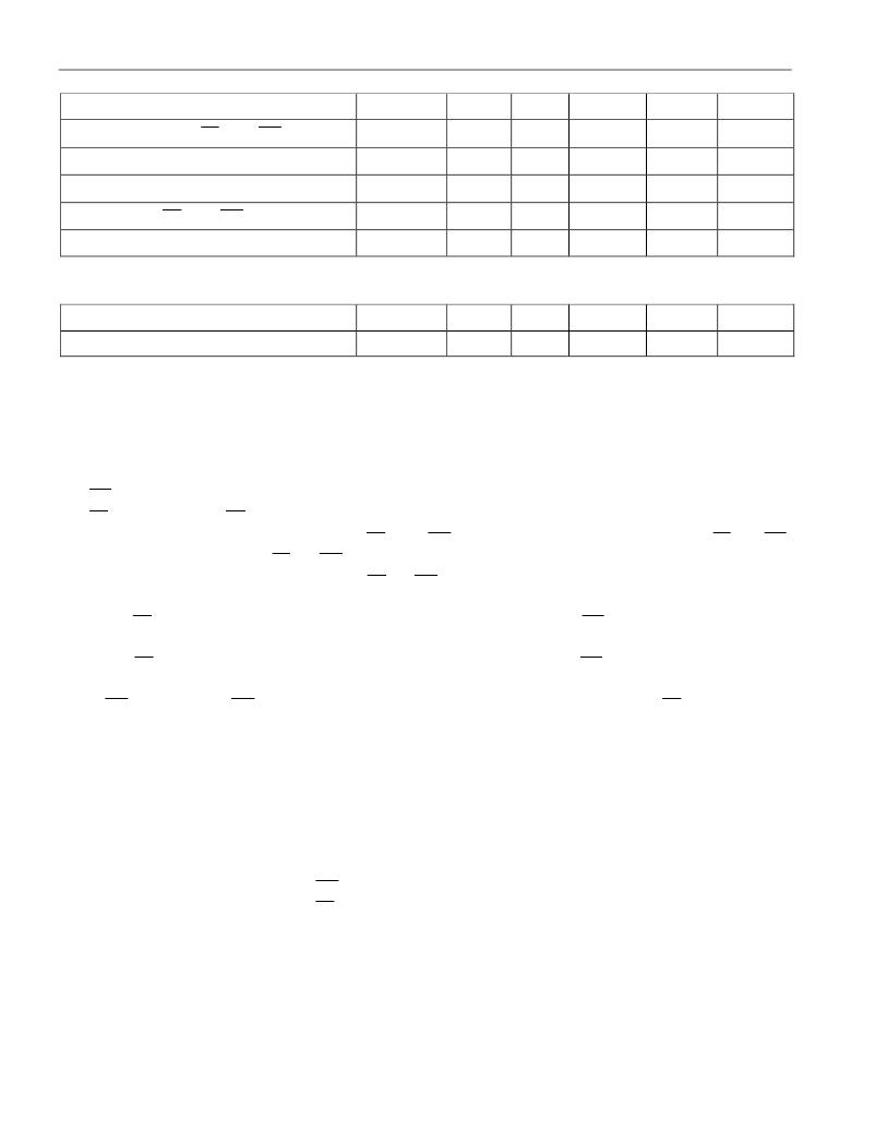
�DS1230W�
�POWER-DOWN/POWER-UP� TIMING�
�(T� A� :� See� Note� 10)�
�PARAMETER�
�V� CC� Fail� Detect� to� CE� and� WE� Inactive�
�SYMBOL�
�t� PD�
�MIN�
�TYP�
�MAX�
�1.5�
�UNITS�
�μ� s�
�NOTES�
�11�
�V� CC� slew� from� V� TP� to� 0V�
�V� CC� slew� from� 0V� to� V� TP�
�V� CC� Valid� to� CE� and� WE� Inactive�
�V� CC� Valid� to� End� of� Write� Protection�
�t� F�
�t� R�
�t� PU�
�t� REC�
�150�
�150�
�2�
�125�
�μ� s�
�μ� s�
�ms�
�ms�
�(T� A� =� +25� °� C)�
�PARAMETER�
�Expected� Data� Retention� Time�
�SYMBOL�
�t� DR�
�MIN�
�10�
�TYP�
�MAX�
�UNITS�
�years�
�NOTES�
�9�
�WARNING:�
�Under� no� circumstance� are� negative� undershoots,� of� any� amplitude,� allowed� when� device� is� in� battery�
�backup� mode.�
�NOTES:�
�1.� W� E� is� high� for� a� Read� Cycle.�
�2.� OE� =� V� IH� or� V� IL� .� If� OE� =� V� IH� during� write� cycle,� the� output� buffers� remain� in� a� high-impedance� state.�
�3.� t� WP� is� specified� as� the� logical� AND� of� CE� and� WE� .� t� WP� is� measured� from� the� latter� of� CE� or� WE�
�going� low� to� the� earlier� of� CE� or� WE� going� high.�
�4.� t� DH� ,� t� DS� are� measured� from� the� earlier� of� CE� or� WE� going� high.�
�5.� These� parameters� are� sampled� with� a� 5� pF� load� and� are� not� 100%� tested.�
�6.� If� the� CE� low� transition� occurs� simultaneously� with� or� latter� than� the� WE� low� transition,� the� output�
�buffers� remain� in� a� high-impedance� state� during� this� period.�
�7.� If� the� CE� high� transition� occurs� prior� to� or� simultaneously� with� the� WE� high� transition,� the� output�
�buffers� remain� in� high-impedance� state� during� this� period.�
�8.� If� WE� is� low� or� the� WE� low� transition� occurs� prior� to� or� simultaneously� with� the� CE� low� transition,�
�the� output� buffers� remain� in� a� high-impedance� state� during� this� period.�
�9.� Each� DS1230W� has� a� built-in� switch� that� disconnects� the� lithium� source� until� V� CC� is� first� applied� by�
�the� user.� The� expected� t� DR� is� defined� as� accumulative� time� in� the� absence� of� V� CC� starting� from� the�
�time� power� is� first� applied� by� the� user.�
�10.� All� AC� and� DC� electrical� characteristics� are� valid� over� the� full� operating� temperature� range.� For�
�commercial� products,� this� range� is� 0� °� C� to� 70� °� C.� For� industrial� products� (IND),� this� range� is� -40� °� C� to�
�+85� °� C.�
�11.� In� a� power-down� condition� the� voltage� on� any� pin� may� not� exceed� the� voltage� on� V� CC� .�
�12.� t� WR1� and� t� DH1� are� measured� from� W� E� going� high.�
�13.� t� WR2� and� t� DH2� are� measured� from� CE� going� high.�
�14.� DS1230� modules� are� recognized� by� Underwriters� Laboratories� (UL)� under� file� E99151.�
�8� of� 10�
�发布紧急采购,3分钟左右您将得到回复。
相关PDF资料
DS1230YP-100+
IC NVSRAM 256KBIT 100NS 34PCM
DS1245AB-120IND+
IC SRAM NV 128KX8 5.25V 32-DIP
DS1245W-100IND+
IC NVSRAM 1MBIT 100NS 32DIP
DS1245Y-70IND+
IC NVSRAM 1MBIT 70NS 32DIP
DS1249AB-85IND#
IC NVSRAM 2048KBIT 85NS 32DIP
DS1249W-100IND#
IC NVSRAM 2MBIT 100NS 32DIP
DS1249Y-70IND#
IC NVSRAM 2MBIT 70NS 32DIP
DS1250AB-70IND+
IC NVSRAM 4MBIT 70NS 32DIP
相关代理商/技术参数
DS1230WP-150-IND
制造商:DALLAS 制造商全称:Dallas Semiconductor 功能描述:3.3V 256k Nonvolatile SRAM
DS1230Y
制造商:DALLAS 制造商全称:Dallas Semiconductor 功能描述:256k Nonvolatile SRAM
DS1230Y/AB
制造商:未知厂家 制造商全称:未知厂家 功能描述:256K Nonvolatile SRAM
DS1230Y_10
制造商:DALLAS 制造商全称:Dallas Semiconductor 功能描述:256k Nonvolatile SRAM
DS1230Y-100
功能描述:NVRAM 256k Nonvolatile SRAM RoHS:否 制造商:Maxim Integrated 数据总线宽度:8 bit 存储容量:1024 Kbit 组织:128 K x 8 接口类型:Parallel 访问时间:70 ns 电源电压-最大:5.5 V 电源电压-最小:4.5 V 工作电流:85 mA 最大工作温度:+ 70 C 最小工作温度:0 C 封装 / 箱体:EDIP 封装:Tube
DS1230Y-100+
功能描述:NVRAM 256k Nonvolatile SRAM RoHS:否 制造商:Maxim Integrated 数据总线宽度:8 bit 存储容量:1024 Kbit 组织:128 K x 8 接口类型:Parallel 访问时间:70 ns 电源电压-最大:5.5 V 电源电压-最小:4.5 V 工作电流:85 mA 最大工作温度:+ 70 C 最小工作温度:0 C 封装 / 箱体:EDIP 封装:Tube
DS1230Y-100IND
制造商:DALLAS 制造商全称:Dallas Semiconductor 功能描述:256k Nonvolatile SRAM
DS1230Y-100-IND
制造商:DALLAS 制造商全称:Dallas Semiconductor 功能描述:256k Nonvolatile SRAM